The thin green line
The ever increasing demand for greener power sources will result in the need for tools that can elucidate the chemical properties of ultra thin films and interfaces. Here,Tim Nunney and Richard White tell us how x-ray photoelectron Spectroscopy is the technique of choice for such a task
The ever increasing demand for greener power sources will result in the need for tools that can elucidate the chemical properties of ultra thin films and interfaces. Here,Tim Nunney and Richard White tell us how x-ray photoelectron Spectroscopy is the technique of choice for such a task

In order to ensure product viability and efficiency it is vital to ensure precise control of surface, thin film and interface composition. The majority of modern devices require a combination of conductive, semi conductive and insulating layers, engineered to deliver particular physical, chemical and electrical properties. During the fabrication process, deviations from the desired chemistry can occur. This is most likely to happen at the crucial interfacial regions where precise chemical engineering meets its greatest challenges. The finished device may also have to be analysed for compositional homogeneity across the surface, to identify defects that could have an adverse impact upon performance and lifetime.
Scientists and engineers working on the latest thin film devices have benefited from the recent developments in spectrometer hardware and software design that have made the unique capabilities of x-ray photoelectron spectroscopy (XPS) more accessible. Due to its extreme surface sensitivity XPS is able to deliver crucial insight by providing characterisation on the nm scale for ultra thin films and interfaces. It can be difficult to maintain accuracy within these limits but improvements within instrumentation and analytical capabilities have resulted in XPS becoming an essential component of the engineer's toolkit.
|
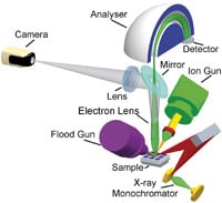
A schematic of the internal configuration of the Thermo Scientific K-Alpha, showing the principal components of a modern XPS spectrometer. The sample is irradiated with monochromatic X-rays, and the resultant photoelectrons are collected by a transfer lens. The photoelectrons are selected based on their kinetic energy by the hemispherical analyser, and collected at the detector. The low energy electron flood gun facilitates the analysis of insulating materials, and the ion gun permits sample cleaning and composition depth profiling. |
Thin film solar cell and fuel cell design and fabrication are reliant on materials engineering on the nm scale; it is therefore vital that techniques that can achieve chemical characterisation on the same scale are available. Here we look at the characterisation requirements for two thin film components, the copper indium gallium (di)selenide (CIGS) solar cell, and the proto exchange membrane fuel cell, (PEMFC). These devices are the latest in current thin film fabrication technology in their respective fields.
XPS data has been widely published for more than 50 years with the technique gaining increasing commercial momentum over the past 40 years. P.D. Innes is credited with recording the first XPS spectrum in 1907 but the real 'father' of XPS as an analytical technique is considered to be Kai Siegbahn who produced the first high-resolution spectrum of sodium chloride in 1954. By the late sixties he had performed a wide ranging study which proved the value of the technique. In 1969 he cooperated with Hewlett-Packard in the USA to produce the first commercial XPS instrument. In recognition of his work in the field of surface analysis Siegbahn received the Nobel Prize for Physics in 1981. To emphasise the fact that XPS provides a method for the chemical characterisation of a surface, Siegbahn referred to the technique as ESCA (electron spectroscopy for chemical analysis), a term which continues to be used alongside the term XPS1.
As the name implies, XPS relies upon the photoelectric effect, in which an x-ray photon removes an electron from an atom located in the surface region of the sample to be analysed. A particular electron will only be emitted provided that the photon has energy in excess of the electron's binding energy to the nucleus. The remaining energy imparted by the photon manifests itself as the emergent electron's kinetic energy. In an XPS spectrometer, it is the kinetic energy of the photoelectron that is measured as it leaves the surface. This process is described simply by the following equation:
Kinetic energy (KE) = Photon energy (h?) – Binding energy (BE)
Typically an X-ray source of a known energy (e.g. Al Ka radiation h? = 1486.6eV) is used in the excitation. This allows the BE of the emergent electron to be easily calculated by rearranging the above equation. Principally the binding energy of the photoelectron is dependent on the identity of the parent atom and it's orbital. Basic interpretation of wide scan survey data which is collected by scanning the analyser through the full range of accessible kinetic energies – the accessible range being dependent on the photon energy – can lead to quantitative determination of the surface elemental composition, with the inclusion of all elements heavier than He. To the first approximation, quantification of the data is achieved by the application of elemental and transition dependent matrix factors during data processing, which removes the need for the use of external calibration standards. Refinements to these factors which take into account the attenuation length of the photoelectron and its kinetic energy lead to an improvement in the accuracy of quantification. These factors are generally supplied by the instrument data system and lead to the detection limit of the technique being about 0.1 atomic%. This elemental information is useful; however the real strength of XPS lies in the fact that the chemical environment of the emitting atom induces subtle changes in binding energy of the photoelectron. As a consequence of this effect, detailed high resolution XPS data sets also contain valuable chemical state information.
|
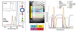
Examples of XPS data. (A) A C1s high resolution spectrum of PET. The colour coding of the peaks relates to the highlighted chemistry in the molecule. The inset is the survey spectrum from the same sample. (B) An XPS image, showing a concentration map overlaid on an optical image, showing an etched area of a patterned wafer. (C) A depth profile of a multilayer sample. |
The basic components of an XPS spectrometer include an X-ray source, electron energy analyser and detection system. Within the XPS spectrometer the emitted photoelectrons need to travel a considerable distance before they reach the detector. To ensure that energy losses due to collisions with gas molecules are kept to a minimum, XPS spectrometers need to be operated under ultra-high vacuum conditions, typically 1x10⁻⁷ mbar or better. Any solid sample that is compatible with these conditions can be analysed, and requires little or no prior sample preparation.
XPS spectrometers are available in a number of forms, from highly configurable multi-technique platforms to dedicated, fully automated spectrometers. Figure 1 shows a schematic illustrating a typical XPS system configuration including components such as a low-energy electron flood source for insulator analysis, an argon ion source for depth profiling applications, and a camera system for aligning the sample with the analysis position.
When considered relative to other electron microscopy techniques, XPS has comparatively poor lateral resolution; however this is mitigated by its extreme surface sensitivity which results in a vertical depth resolution on the nm scale (typically less than 10nm). The surface sensitivity of XPS is often mistakenly attributed to X-ray penetration depth or the analysis geometry. In reality the surface specificity of XPS is a consequence of the strong interaction of photoelectrons with condensed matter. When X-rays strike a solid, they penetrate the material to a great depth causing photoemission along the whole of their path of travel. In contrast, as the emitted photoelectrons travel through the material, they undergo inelastic collisions with other particles in the solid. Only photoelectrons originating at, or close, to the surface (within the top 5 to 10 nm, depending on the material) have a reasonable probability of escaping without energy loss. The XPS spectrum consists of sharp peaks on a broad background. Electrons generated close enough to the surface that can escape without energy loss contribute to the peaks while those that escape having lost some energy through the aforementioned inelastic collisions contribute to the spectrum background.
|
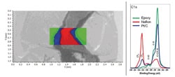
Optical image of the prepared MEA sample, with an overlay of the XPS map data, and average C1s spectra from the three identified phases (Green – epoxy, blue – Pt on carbon black, red – Polymer electrolyte). Some fluorine contamination from the membrane is visible in the Pt/C section. |
The simplest form of XPS analysis is a single point analysis, as shown in Figure 2A, such measurements can be made from areas down to about 10µm in diameter. Imaging XPS is possible by using either parallel detection systems or stage mapping (Figure 2B). Current state of the art capabilities result in elemental or chemical state images having a resolution of the order of 3µm. If XPS measurements are interleaved with Ar ion beam etch cycles then it is possible to produce a chemical composition depth profile (Figure 2C). This makes it possible to determine the composition of films that are much thicker than the escape depth of the electrons.
The range of application areas that XPS addresses is extensive, encompassing both academic and industrial R&D2-6. With the recent explosion of manufacturing processes that utilise thin film fabrication methods XPS is seeing increasing adoption for quality assurance and control purposes. Common uses for XPS are:
• Measuring surface contaminants
• Ultra thin film and oxide thickness measurements
• Characterisation of surface defects, stains and discolorations
• Measuring effectiveness of surface preparation treatments
• Surface composition of powders and fibres
• Chemical characterisation of plasma modified polymer materials
• Measurement of coating thickness and conformity
• Composition depth profiling for multilayer and interface analysis.
|
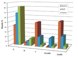
Results from the quantitative analysis from the three regions of the sample. |
Case study 1: Characterisation of Fuel Cell Components
For our first example of how XPS is used in modern thin film analysis, we consider the analysis of a proton exchange membrane fuel cell (PEMFC). These devices are currently being developed for both stationary and transport applications, such as remote telecommunications base stations and motor vehicles. PEM fuel cells have several advantages over current solid oxide fuel cells (SOFC), including higher conversion efficiencies and considerably lower operating temperatures (typically <100°C), leading to improved start-up performance.
At the heart of the fuel cell is a membrane electrode assembly (MEA). The MEA has layers of platinum in carbon black, which catalyses the reaction of hydrogen and oxygen. A polymer electrolyte (typically Nafion) is used to separate the anode and cathode electrodes. In MEA manufacture or development, the aim is to maximise the surface area of platinum that is electrically connected to the conducting support; loss of surface area decreases the efficiency of the device. Platinum loss can occur when high currents effectively corrode the carbon-black support, liberating the active metal and allowing it to migrate to the adjacent polymer electrolyte. Additionally, the presence of platinum in the Nafion hinders hydrogen ion mobility in the electrolyte. The purpose of the analysis is to determine if the platinum has migrated from the catalytically active layers into the adjacent Nafion electrolyte.
The MEA layers are typically too thick for conventional XPS depth profiling and so sectioning was required before the XPS analysis could commence. A simple 90° cross-section would reveal layers that would be too thin for XPS analysis, making it impossible to detect the subtle diffusion of the platinum from one layer to another. The solution to this was to mount the sample in epoxy and to use ultra-low angle microtomy (or ULAM) to cross-section the MEA at an angle of 1° or 2°. ULAM sectioning effectively stretches the available analysis area, making the dimensions several times larger than the x-ray probe size, which allows the analyst to obtain effective depth information by imaging the section.
|
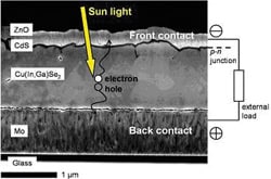
Scanning electron micrograph of a Cu(In,Ga)Se2 solar cell (cross-section) and its mode of operation. |
Figure 3 shows the C 1s region of the XPS spectrum from the Nafion and epoxy areas of the sample. The Nafion spectrum has a strong peak associated with CF2 groups in the polymer. It also has a peak at lower binding energy associated with adventitious carbon contamination. The epoxy spectrum has components associated with aromatic, aliphatic and carboxyl type carbon bonding. From the mapping data in Figure 3 it was possible to determine the elemental composition of the MEA-ULAM sample at different areas on the surface, as shown in Figure 4. Fluorine and sulphur were observed in the catalyst layer; these are expected since a small amount of Nafion, which contains sulphur, was mixed into the platinum-carbon layer during manufacture. Although sulphur is not a contaminant in the platinum layer, these results demonstrate the capability of the XPS tool to detect potential contaminants at low concentration.
Despite the concentration of catalytically active Pt being less than 0.5 at.%, a high quality, high signal-to-noise spectrum was acquired from the catalyst layer. As hoped no Pt was detected in middle of the Nafion layer suggesting minimal Pt migration.
Case study 2: Compositional analysis of a CIGS solar
cell
For our second example we will look at an XPS analysis of a thin film solar cell. Solar cells based on Cu(In,Ga)Se2 (CIGS) thin films have demonstrated excellent efficiencies and offer the potential of a low-cost alternative to bulk, silicon-based, solar cells. They consist of a thin-film stack on a substrate (typically glass), as shown in Figure 5. Molybdenum and zinc oxide layers form the electrical contacts, the p-type CIGS film acts as the sunlight absorber layer, with a thin n-type CdS layer forming a p-n junction. The most common manufacturing methods involve evaporation and/or sputter deposition of the components onto a substrate. For the CIGS layer, the Cd, In and Ga are deposited first, before the film is exposed to selenium vapour, which reacts with the metals in order to establish the final film composition.
|
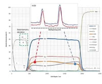
Depth profile of the CIGS solar cell. Variation in the In3d peak position is indicative of the changing chemical environment through the CIGS layer. The thin CdS layer is also apparent at the ZnO-CIGS interface. |
One of the major challenges in producing these devices is to control the CIGS film composition; hence reproducibility of layers in commercial volumes has been problematic. This is critical to performance, as the electrical properties of the cell are dependent on the exact composition of the various layers. Depth profiling with XPS can determine both the composition through the structure, and the nature of the chemistries formed at the interfaces. This is essential for understanding how to control the band gap to provide efficient operation of the light adsorbing layer.
The analysis in this particular example takes the form of an XPS depth profile acquisition. As with most depth profiles, argon ions were used to generate the sputter crater. The depth concentration profile results can be seen in Figure 6. The depth calibration scale was confirmed using the cross-section SEM image as a reference.
The depth profile clearly follows the expected structure of the solar cell; the transparent ZnO front contact layer, the thin n-type CdS layer, the light adsorbing, p-type CIGS layer, and finally the Mo back contact. The profile highlights the composition gradient of gallium and indium within the CIGS layer. Controlling the composition of this gradient is of critical importance as it is known to influence the band gap of the material and therefore the overall efficiency of the device. The quality of this profile demonstrates the capability of modern day XPS spectrometers to produce composition profiles from complex multi-component films while maintaining excellent depth resolution throughout.
The profile also highlights a change in stoichiometry within the ZnO layer as the n-type CdS layer is approached. This is likely to be caused by a reduction of the ZnO layer as it chemically interacts with the CdS layer. This interfacial artefact is likely to have some significance to overall device performance. Further inspection of the data set reveals subtle chemical differences within the absorber layer. The inset showing the In3d XPS transition confirms that the indium oxidation state changes with increasing Ga concentration. This will have a direct influence on the electronic structure and therefore the band gap of the device. The analysis can be extended to look for dopants, such as sodium, in the layers which can further enhance (or be detrimental) to the performance of the device.
The ever increasing demand for new thin film devices for cleaner power sources will result in the need for tools that can elucidate the chemical properties of ultra thin films and interfaces. A single technique can not often meet all the analysis requirements, and it is therefore often the case that a complementary approach involving several techniques is required. Energy dispersive spectroscopy (EDS) and Raman are both obvious candidates to be included within this portfolio as they add rapid composition mapping and molecular contrast. The examples given within this article demonstrate why multi-technique investigations can benefit greatly from XPS analysis.
The Authors: Tim Nunney & Richard White Richard is the sales and marketing manager for surface
analysis products at Thermo Fisher Scientific, and Tim is the product
manager for the Thermo Scientific K-Alpha XPS system Contact:e:tim.nunney@thermofisher.com

